
01
Crystal Growth
Material preparation and crystal-growth requirements

About Power Wafertech Group
A unified view of our product focus, development history, manufacturing workflow, quality approach and customer collaboration model.
Company Overview
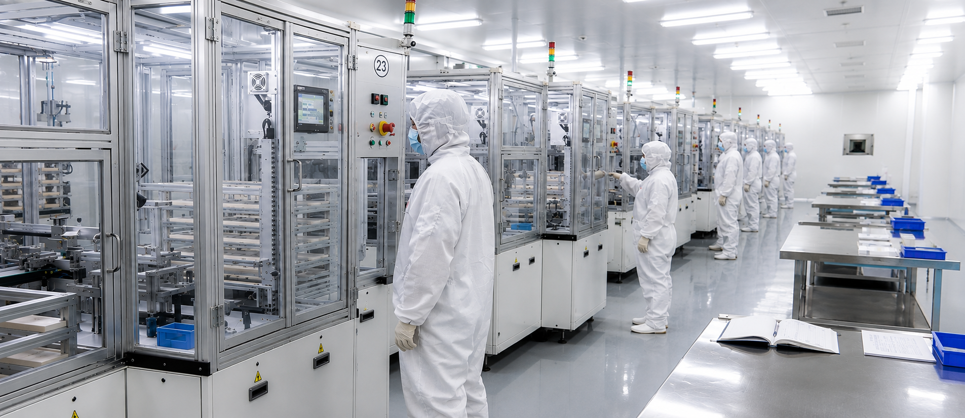
Power Wafertech Group focuses on compound semiconductor substrates, epitaxial wafers and specialty wafer requirements. Our role is to connect material understanding, specification review, controlled processing and engineering communication across the customer program lifecycle.
We support international customers through clearly defined requirements, manufacturing coordination, documentation and responsive technical communication. Specific operating locations, certifications and service coverage should be published only after formal verification.
Technology & Manufacturing
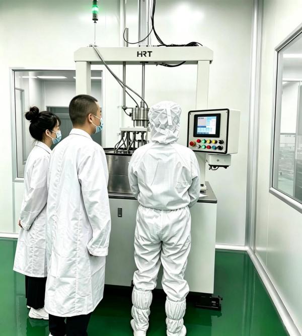
The exact process sequence depends on product and project scope. This overview shows how material, wafer, epitaxy, fabrication and characterization activities connect.
01
Material preparation and crystal-growth requirements
02
Geometry, surface and dimensional processing
03
HVPE / MBE / MOCVD scope confirmed by product
04
Optional downstream processing per agreed scope
05
Inspection, measurement and documentation
Wafer Services
We will verify the applicable service scope, material matching performance, dimensional specifications and qualification standards on a case-by-case basis for all customer enquiries.
Wafer reclaim、metallization
Photolithography、etching
Thin films、ion implantation
Epitaxy、custom development
Quality & Inspection
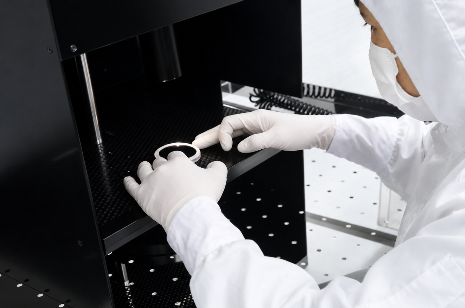
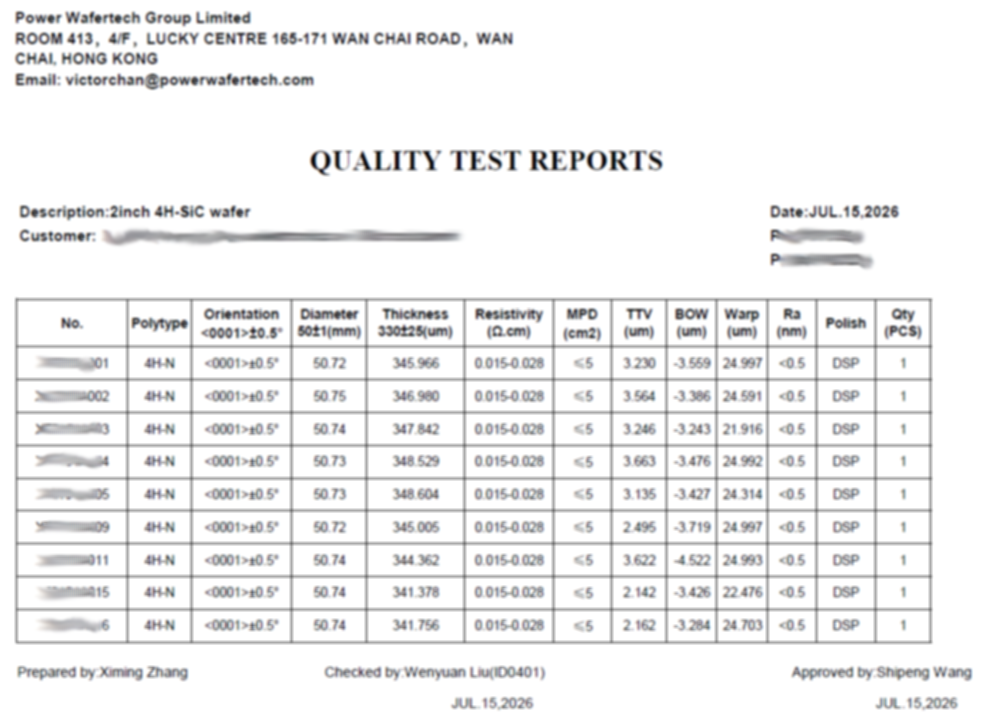
Quality expectations are aligned at specification review and supported through incoming, in-process and outgoing controls. Available reports, traceability fields and packaging options are confirmed per product and order.
Quality Test Reports
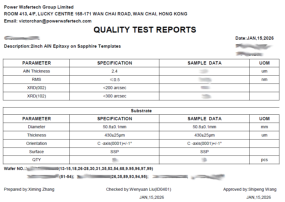
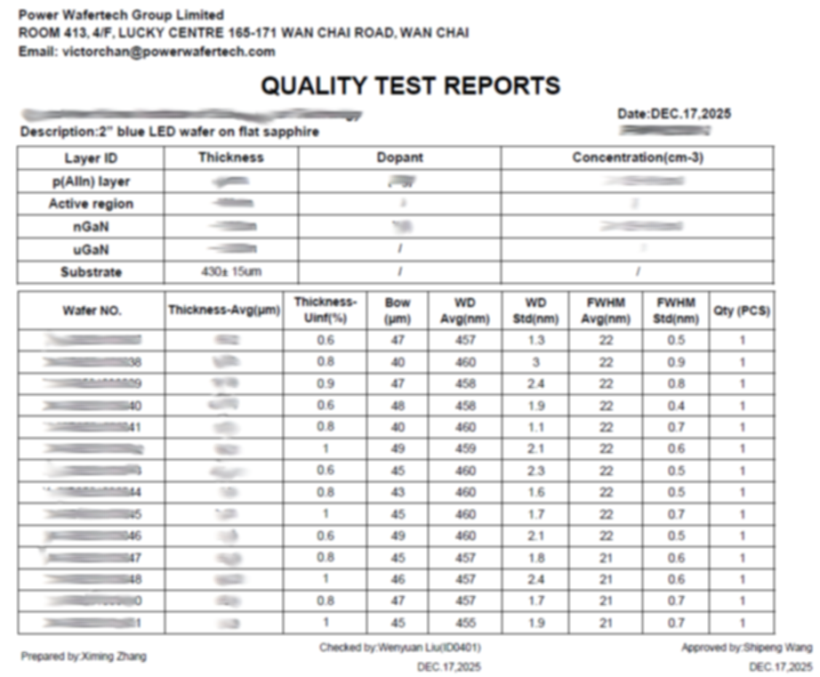
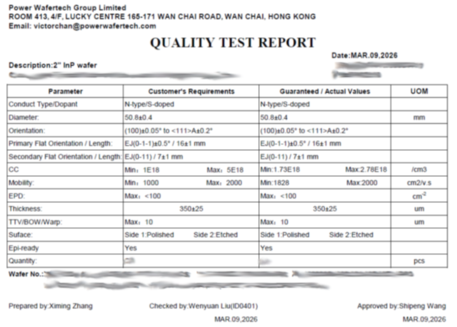
Collaboration Evidence
The examples below are anonymized content structures. Customer names, quantitative results and project details must be added only with approval.
Industry Program
Specialty substrate specification for a defined device process
Specification review, evaluation coordination and repeat-order planning
Research Program
Small-volume wafers available for material characterization and process feasibility evaluation.
Flexible quantity review, documentation alignment and technical communication
Application Development
Custom geometry and surface requirements for an emerging application
Feasibility review, custom processing scope and qualification planning
Facilities & Global Support
View each site's business scope. Facility information is documented subject to formal validation.
Base 01
Crystal and material preparation
Base 02
Slicing, grinding and polishing
Base 03
Epitaxy, deposition and metrology
Base 04
Special formats, QA and program support
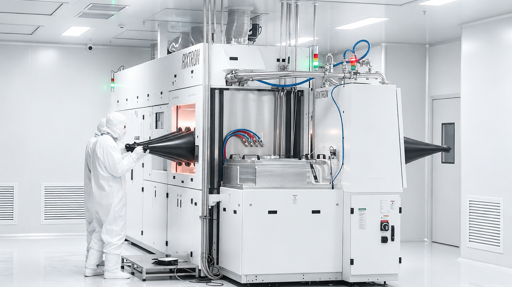
Verified facility details to be added
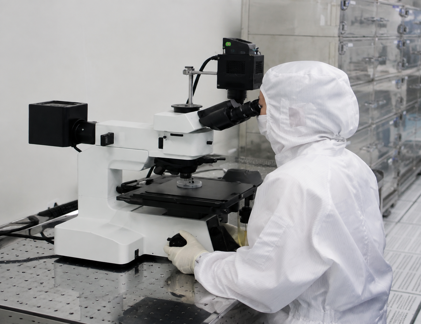
Verified equipment and test scope to be added
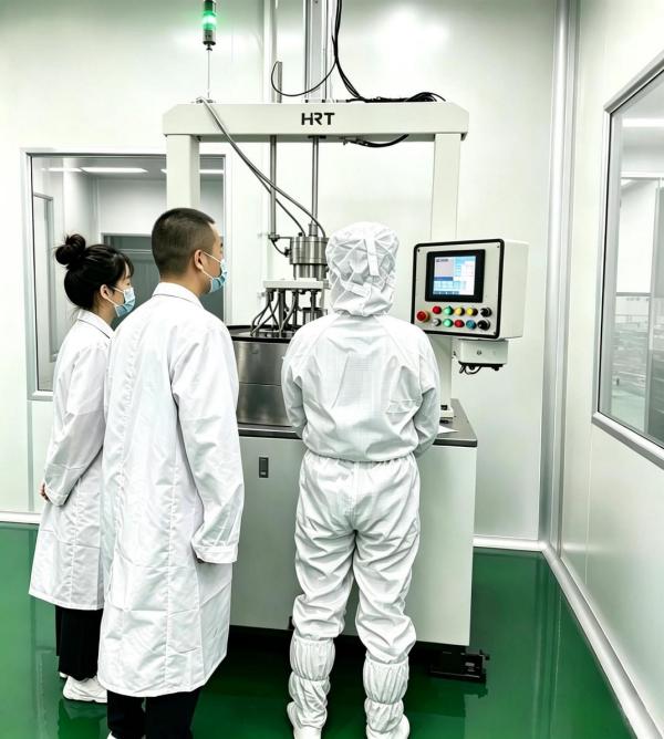
Approved certificates and service locations to be added
Work with Power Wafertech
Explore our wafer portfolio or discuss a material, processing or program requirement with our team.


