

The silicon wafer industry is the most reliable early indicator of semiconductor manufacturing activity, because wafer area entering a fab is a physical quantity that cannot be inflated by pricing or by inventory accounting. The latest figures from the SEMI Silicon Manufacturers Group show an industry not just recovering, but broadening: growth is no longer confined to advanced logic and memory.
For research groups, pilot lines, and device manufacturers buying silicon substrates, the practical question raised by these numbers is about lead time and qualification planning. This article sets out the data, explains the supply-side constraint behind it, and translates both into a procurement checklist.
1. The headline numbers
| Period | Global shipments (MSI) | Year on year | Quarter on quarter | Context |
|---|---|---|---|---|
| Q2 2025 | 3,327 | — | — | Baseline quarter |
| Q1 2026 | 3,275 | +13.1% | -4.7% | Sequential decline consistent with normal seasonality |
| Q2 2026 | 3,573 | +7.4% | +9.1% | Strongest sequential gain of the current cycle |
| 2026 full year (SEMI forecast) | — | +5.2% | — | Growth expected to continue through 2028 |
| 2028 (SEMI forecast) | ~15,485 | — | — | Projected new industry record |
MSI denotes million square inches of shipped wafer area, including polished wafers supplied to device makers, virgin test wafers, and epitaxial silicon. Because the metric records substrate area entering fabrication rather than the value of finished devices, it tends to move ahead of revenue and provides one of the earlier signals available on manufacturing intent.
Why the Q2 jump matters: a 9.1% sequential increase is unusual for a single quarter. It indicates that fabs are not merely replenishing inventory — they are loading wafers into production. Combined with 7.4% year-on-year growth, the data points to genuine capacity expansion rather than a restocking bounce.
2. AI demand has broadened beyond logic and memory
The most important qualitative change in the commentary accompanying these figures is the scope of AI demand. Through 2024 and much of 2025, AI-driven wafer consumption was concentrated in advanced logic accelerators and high-bandwidth memory. In 2026, SEMI attributes growth to AI-related demand extending into power devices, photonics, and other adjacent categories.
This broadening is structural rather than incidental. A data center is not only a collection of accelerators; it requires power conversion at every level from the grid connection to the point of load, optical transceivers and their photodetectors and drivers, network switching silicon, timing components, and the analogue and control electronics that surround all of it. Each of those categories consumes silicon substrate area — much of it on mature nodes and smaller diameters.

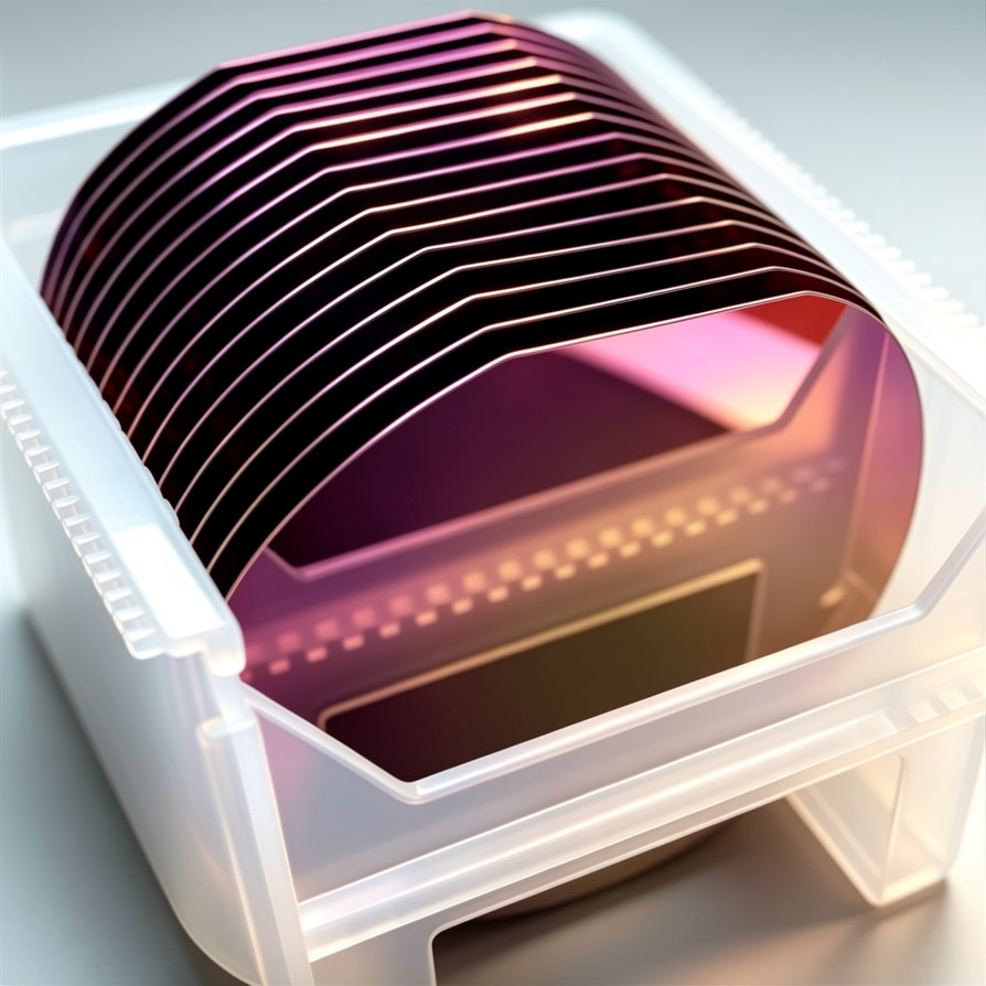
Fig. 1 — Silicon epitaxial wafer. Epitaxial silicon remains the substrate of choice where defect-free surfaces and controlled resistivity profiles are required.
The intensity of AI demand is also higher per unit of function than conventional computing. Industry analyses indicate that AI servers consume substantially more 300 mm wafer area per server than general purpose servers, and that memory products built for AI workloads consume multiples of the wafer area of conventional memory at equivalent capacity. The consequence is that AI now influences substrate demand across the diameter range, not only at the leading edge.
3. Supply cannot respond quickly
Silicon wafer manufacturing is capital intensive and slow to expand. A new crystal growth and wafer processing line typically requires eighteen to twenty-four months from equipment order to meaningful output, followed by a customer qualification period that is longer still for 300 mm products with tight defect, flatness, and surface quality requirements. Short-term demand increases therefore cannot be met with short-term supply.
Several analyses of the current cycle conclude that announced incremental supply covers only about half of projected incremental demand over the coming year, implying that tight conditions could persist into 2027. Whether or not that specific ratio holds, the direction is consistent with the observed behaviour of major suppliers, who have directed capital expenditure toward high-value 300 mm capacity while actively limiting expansion of legacy 6-inch and 8-inch lines.
4. Mature diameters are the quiet squeeze
The most consequential effect for many buyers is at smaller diameters. Because leading suppliers have prioritised 300 mm investment, capacity additions at 6-inch and 8-inch have been limited, and some older lines have been retired. At the same time, demand for mature-node wafers is rising: automotive and industrial semiconductor demand is recovering after an extended inventory correction, power devices are growing on the back of electrification and AI infrastructure, and research and pilot production consumption continues to expand.
Consumer markets present a partial offset. Memory price pressure has constrained PC and smartphone builds, which limits demand in some high-volume categories. The net effect is a recovery that is uneven by diameter, process technology, and end market — which is precisely the environment in which buyers of smaller-diameter and specialty wafers encounter the longest lead times.
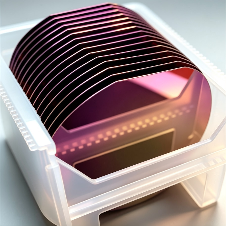
Fig. 2 — Thermally oxidized silicon wafer. Oxide and other film-bearing wafers add process steps ahead of use, making lead time planning more important.
5. What buyers should do now
A tightening substrate market rewards preparation over negotiation. The following measures consistently reduce risk when lead times extend:
- Qualify a second source before you need one. Qualification cycles run for months; starting only after a supply disruption means accepting whatever is available.
- Freeze the specification, not just the part number. Define orientation, doping type and resistivity range, thickness and total thickness variation, surface finish, and particle limits. Ambiguity in specification is the most common cause of incoming-inspection rejection when supply is tight.
- Order further ahead on non-standard items. Off-axis orientations, high-resistivity float-zone material, custom oxide thicknesses, and non-standard diameters carry the longest lead times and cannot be substituted at short notice.
- Request batch documentation with the shipment. Certificates of analysis, measurement methods, and packaging conditions should be agreed in advance so that lots can be compared objectively.
- Consider packaging and cleanliness requirements explicitly. For research and pilot work, vacuum or nitrogen-purged sealed packaging and cleanroom handling can matter as much as the wafer specification itself, since surface condition determines whether cleaning steps are needed before use.
6. Reading the wafer-area number correctly
One caution applies to interpreting these statistics. Wafer area is not a proxy for semiconductor revenue. Device pricing, factory utilisation, process complexity, die size, and product mix all determine the commercial value produced from each square inch, and a mature-node power device and an advanced logic processor consume very different capital despite starting from the same substrate material.
For buyers, however, the metric is still directly useful: rising wafer area means fabs are loading more material, which means competition for substrate capacity among all customers, including research institutions and small-volume specialty buyers who have limited leverage in an allocation environment.
7. How PWG supports silicon wafer programs
Power Wafertech Group supplies prime, research, and dummy-grade silicon wafers covering 2-inch to 12-inch diameters, in standard and custom orientations, doping types, and resistivity ranges, with epitaxial silicon and thermally oxidized wafers also available. For research and pilot production, the relevant considerations are usually specification accuracy, documentation, and packaging: material is packed under cleanroom conditions with batch-level analysis, and technical support covers substrate selection and cleaning-process adaptation for specific experimental requirements. Teams planning work against tight schedules are advised to confirm specification and lead time before finalising process plans.
Data sources
- SEMI Silicon Manufacturers Group (SMG), quarterly worldwide silicon wafer shipment statistics, Q2 2026 release (3,573 MSI, +7.4% year on year, +9.1% quarter on quarter) and Q1 2026 release (3,275 MSI, +13.1% year on year).
- SEMI SMG commentary on AI-related demand extending to power devices, photonics, and adjacent markets, and on recovery in industrial and automotive demand.
- SEMI forecast of continued shipment growth through 2028 and a projected industry record near 15,485 MSI.
- SUMCO and securities-research commentary on AI-driven wafer intensity and supply-demand balances for mature diameters.
- Market-share and capacity-cycle figures attributed to securities research are directional estimates and vary between sources.
Discuss a substrate requirement with our team
Power Wafertech supplies high-quality semiconductor wafers and epitaxial solutions tailored to your device specifications. Reach out to explore substrate and epiwafer options for your next project.
Contact Our Team