
01
GaN Power Electronics
AlN-on-silicon templates can be used as a buffer platform for GaN-on-Si power devices, including GaN HEMTs and high-efficiency switching devices.

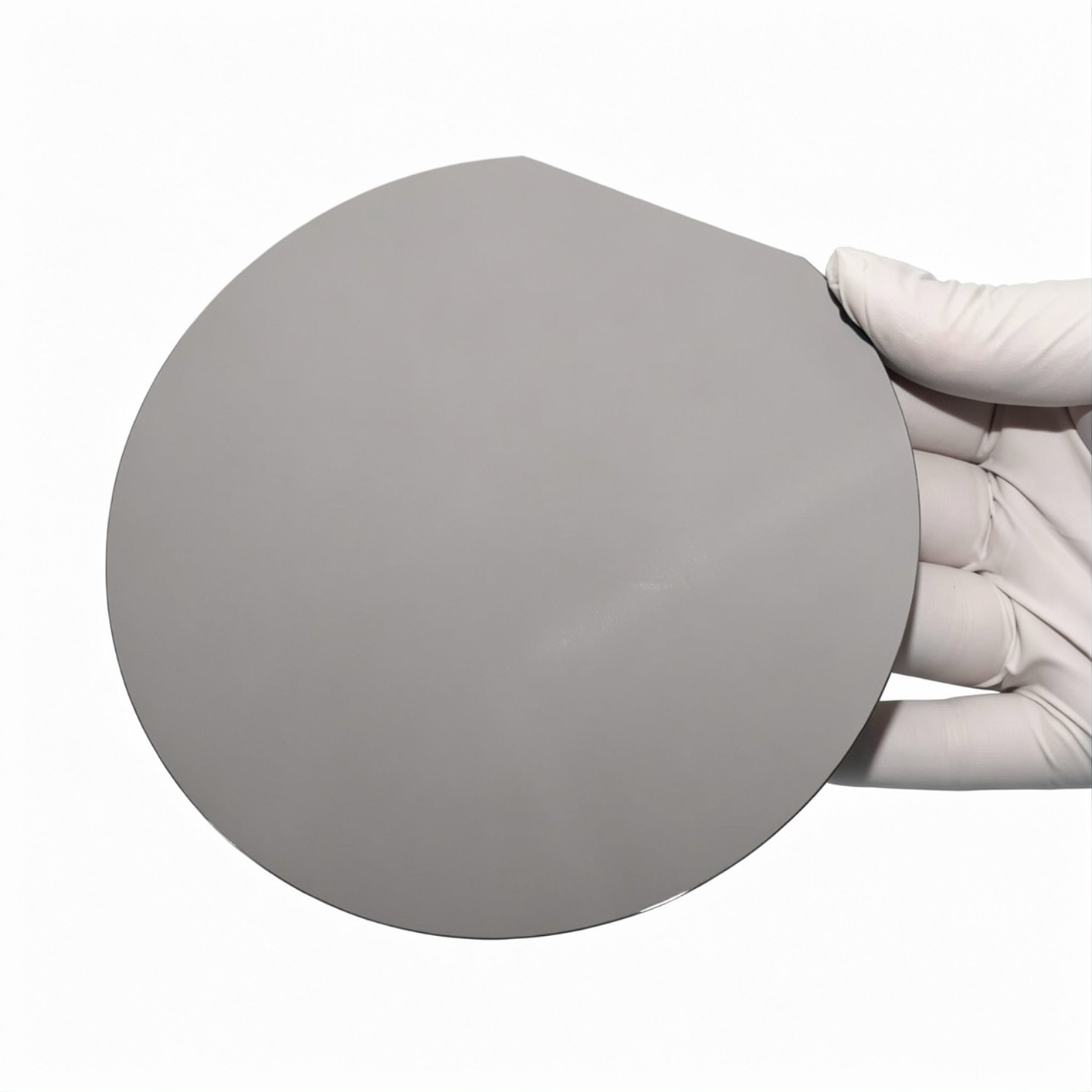
Select a diameter to review the corresponding published specification set.
* Typical specifications; actual values may vary according to wafer size, substrate and growth conditions.
AlN-on-silicon templates can be used as a buffer platform for GaN-on-Si power devices, including GaN HEMTs and high-efficiency switching devices.
AlN-on-silicon templates can also support selected GaN RF and high-frequency device structures, depending on the overall epitaxial design. Typical applications include:
The templates provide a controlled AlN interface for subsequent GaN / AlGaN epitaxial growth, making them suitable for research and development of GaN HEMT structures.
Quick answers on material selection, customization, testing and ordering.
Typical AlN thickness ranges from 50nm to 1μm, and can be customized according to the GaN epitaxial architecture.
Yes. Small quantities and customized specifications can be discussed for research and prototype projects.
Please provide the wafer diameter, silicon orientation, AlN thickness, quantity and target application. We can then recommend a suitable specification and quotation.
Technical Inquiry
Share your material, dimensions, specifications, application or project stage. Our team will review your requirements and respond within one business day.
Engineering-led response
Inquiries are routed to the appropriate technical or commercial team.
Address
No. 1389, Lianmei Road, Lianhua Industrial Zone, Tong’an, Xiamen, Fujian 361100, China
Phone


