GaAs Wafer | Power Wafertech Group

III-V Compound Wafers

GaAs Wafer

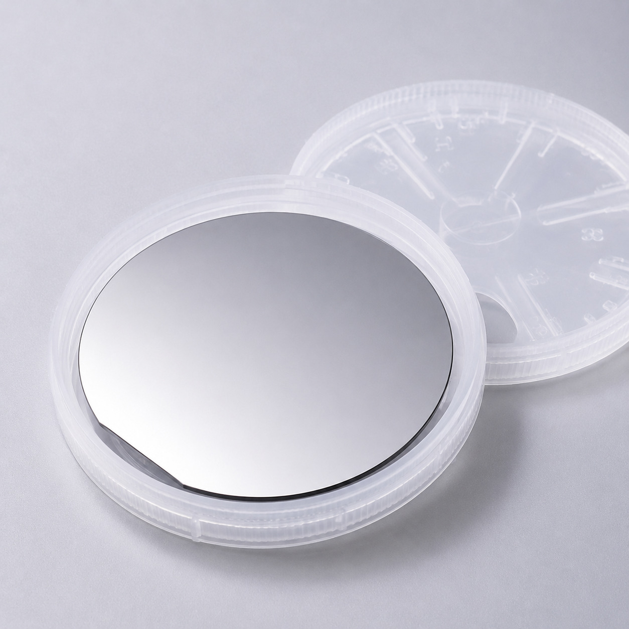
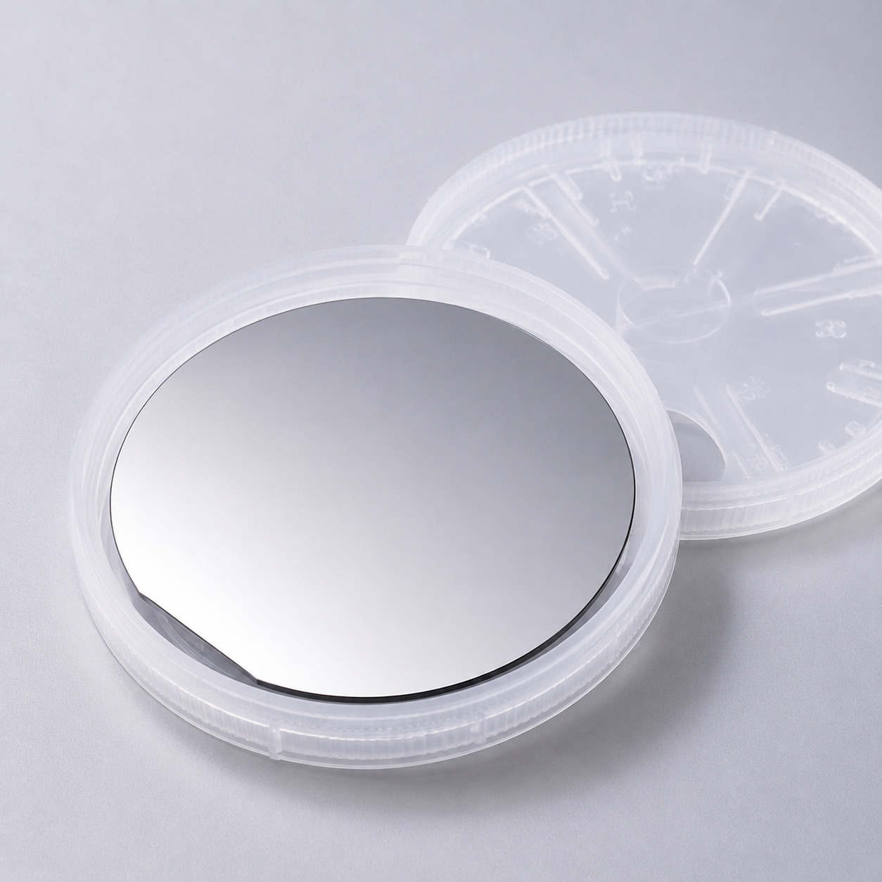
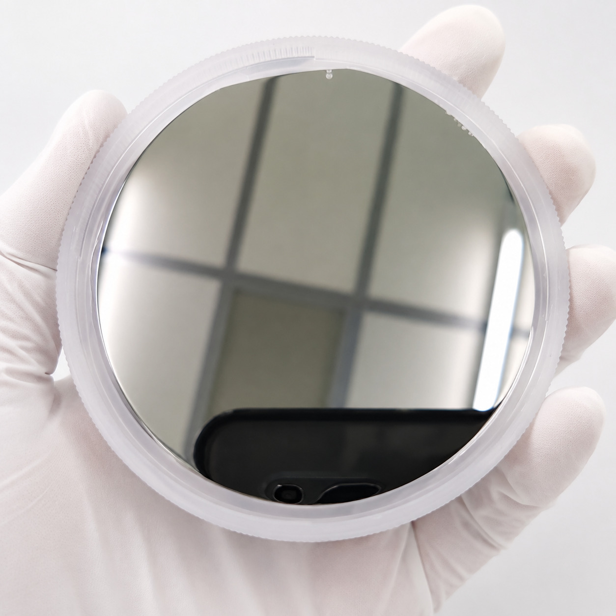
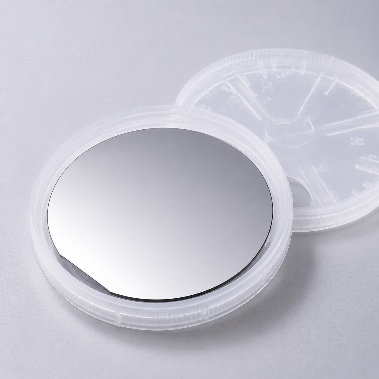
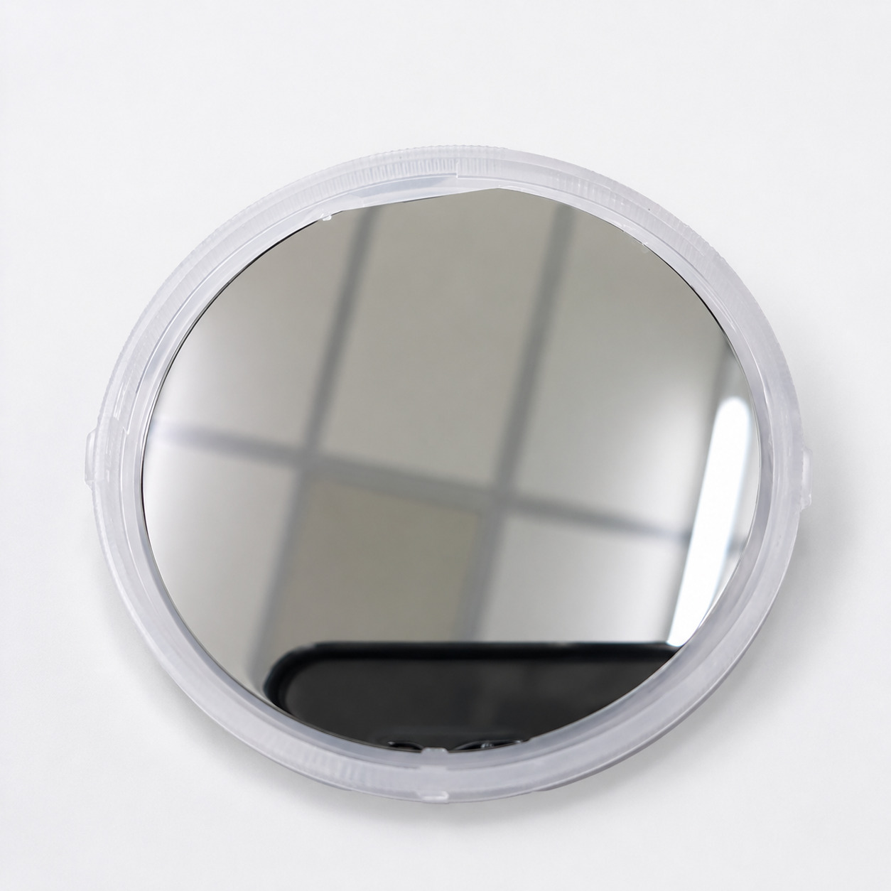
Gallium Arsenide (GaAs) combines a direct bandgap with high electron mobility, making it a widely used substrate material for MMICs, HEMTs, HBTs, VCSELs, laser diodes, LEDs and high-efficiency solar cells. GaAs wafers are available in multiple diameters, crystal orientations and surface finishes.
  • Size 2", 3", 4" and 6"
  • Orientation (100), (111)A and (111)B
  • Conduction type N-type (Si doped), P-type (Zn doped) and Semi-insulating (C doped)
  • Surface finished SSP or DSP, epi-ready
  • Packaging Single wafer cassette, vacuum sealed
Detailed Specifications

Published specifications by wafer diameter.

Select a diameter to review the corresponding published specification set.

Parameter2”(50.8mm) GaAs Substrate
Conduction TypeN-Type
DopantSi
Orientation(100), (111)A, (111)B
Resistivity(1.5–9) × 10⁻³ Ω·cm
Mobility1500–3000 cm²/V·s
EPD≤5000 cm⁻²
Surface FinishSSP / DSP, epi-ready
FlatSEMI standard
PackagingSingle wafer cassette, vacuum sealed
Applications

Where this wafer delivers value

01

RF & Microwave

Semi-insulating GaAs wafers provide electrical isolation and low parasitic effects for high-frequency device fabrication. Typical devices: MMICs HEMTs pHEMTs HBTs Low-noise amplifiers RF power amplifiers Typical applications: 5G / 6G communications Wireless infrastructure Satellite communications Radar RF instrumentation
02

VCSELs & Laser Diodes

Conductive GaAs wafers are widely used as substrates for III-V optoelectronic structures based on AlGaAs, InGaAs and related materials. Typical devices: VCSELs Laser diodes Infrared LEDs Optical sensing devices

03

Photovoltaics

GaAs offers high optoelectronic conversion performance and is used in high-efficiency photovoltaic devices. Typical applications: Space solar cells High-efficiency solar cells Concentrated photovoltaics

04

LED & Optoelectronics

GaAs substrates support the growth of III-V epitaxial structures for red, infrared and other optoelectronic devices.

FAQ

Common questions about this product

Quick answers on material selection, customization, testing and ordering.

Conductive GaAs is commonly used where electrical current injection is required, such as optoelectronic devices. Semi-insulating GaAs provides high electrical resistivity and is widely used for RF and microwave devices.

C-doped semi-insulating GaAs is commonly selected for MMICs, HEMTs, pHEMTs, HBTs and other high-frequency devices.

Conductive GaAs wafers are commonly used as substrates for VCSEL and laser diode epitaxy, with the exact conductivity type depending on the device structure.

Technical Inquiry

Speak to Engineers About Your Wafer Needs

Share your material, dimensions, specifications, application or project stage. Our team will review your requirements and respond within one business day.

Engineering-led response

Inquiries are routed to the appropriate technical or commercial team.

Address

No. 1389, Lianmei Road, Lianhua Industrial Zone, Tong’an, Xiamen, Fujian 361100, China

File Upload
Emailvictorchan@powerwafertech.com Phone+86-592-5633652