
GaSb Wafer | Power Wafertech Group

III-V Compound Wafers

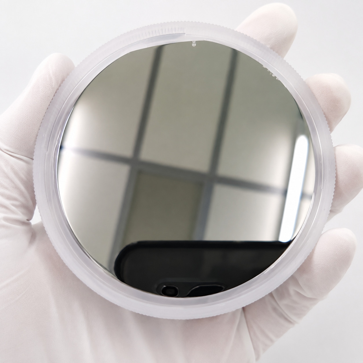
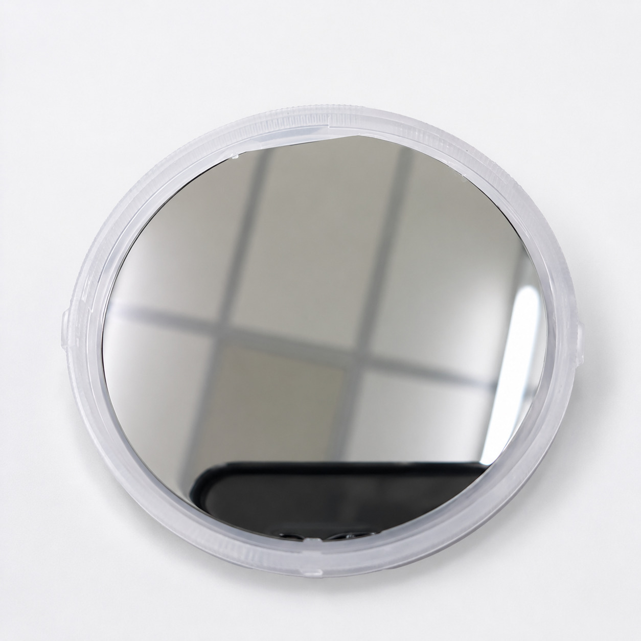
GaSb Wafer

With a lattice constant of approximately 6.096 Å, GaSb (Gallium Antimonide) provides excellent lattice compatibility with antimonide-based materials such as InAs, AlSb and InAsSb, making it an important substrate platform for Type-II superlattice (T2SL) infrared detectors, mid-IR lasers and advanced optoelectronic devices. GaSb wafers are available in multiple diameters, crystal orientations and surface finishes for epitaxial growth and device fabrication.
  • Size 2", 3" and 4"
  • Orientation (100), (111)
  • Conduction type N-type (Te-doped) and P-type (Zn-doped)
  • Surface finish SSP or DSP, epi-ready
  • Packaging Single wafer cassette, vacuum sealed
Detailed Specifications

Published specifications by wafer diameter.

Select a diameter to review the corresponding published specification set.

Parameter2”(50.8mm) GaSb Substrate
Conduction typeN-Type
DopantTe
Orientation(100) / (111)
Thickness500±25um
TTV<10um
Bow<10um
Warp<12um
Mobility2,000–3,500 cm²/V·s
Carrier Concentration(1–20) × 10¹⁷ cm⁻³
EPD≤2,000 cm⁻²
Surface FinishSSP / DSP, epi-ready
FlatSEMI standard
PackagingSingle wafer cassette, vacuum sealed
Applications

Where this wafer delivers value

01

Type-II Superlattice Infrared Detectors

GaSb provides a suitable lattice platform for InAs/GaSb and related Type-II superlattice structures, enabling bandgap engineering across a broad infrared wavelength range. Typical devices: Type-II superlattice (T2SL) detectors MWIR infrared detectors LWIR / VLWIR detectors Infrared focal plane arrays (FPAs) Typical applications: Thermal imaging Infrared sensing Gas detection Spectroscopy Defense and aerospace imaging Recommended substrate: N-type or P-type GaSb according to the epitaxial and device structure.
02

Mid-Infrared Lasers & Photonics

GaSb is an important substrate material for antimonide-based mid-infrared laser and optoelectronic structures. Typical devices: Mid-IR laser diodes IR LEDs Antimonide-based photonic devices Quantum well and superlattice structures Typical applications: Gas sensing Environmental monitoring Medical diagnostics Molecular spectroscopy Recommended substrate: N-type GaSb is commonly selected where an electrically conductive substrate is required for device fabrication.

03

Thermophotovoltaic Applications

GaSb's relatively narrow bandgap makes it suitable for thermophotovoltaic (TPV) cells designed to convert thermal radiation into electrical energy. Typical applications: Waste heat recovery Industrial energy harvesting Thermal-to-electric energy conversion Radioisotope power systems Recommended substrate: P-type GaSb for selected photovoltaic device structures.

FAQ

Common questions about this product

Quick answers on material selection, customization, testing and ordering.

GaSb provides a suitable lattice platform for InAs/GaSb and related Type-II superlattice structures, enabling infrared bandgap engineering through heterostructure design.

Both N-type and P-type GaSb can be used. The appropriate conductivity type depends on the specific T2SL epitaxial and device architecture.

Technical Inquiry

Speak to Engineers About Your Wafer Needs

Share your material, dimensions, specifications, application or project stage. Our team will review your requirements and respond within one business day.

Engineering-led response

Inquiries are routed to the appropriate technical or commercial team.

Address

No. 1389, Lianmei Road, Lianhua Industrial Zone, Tong’an, Xiamen, Fujian 361100, China

File Upload
Emailvictorchan@powerwafertech.com Phone+86-592-5633652