
01
InGaAs/InP
High-speed optical receivers, mmWave HEMTs | Typical Structure: PIN/APD Detector HEMT Channel | Key Properties: High electron mobility Absorption at 1.3-1.55µm

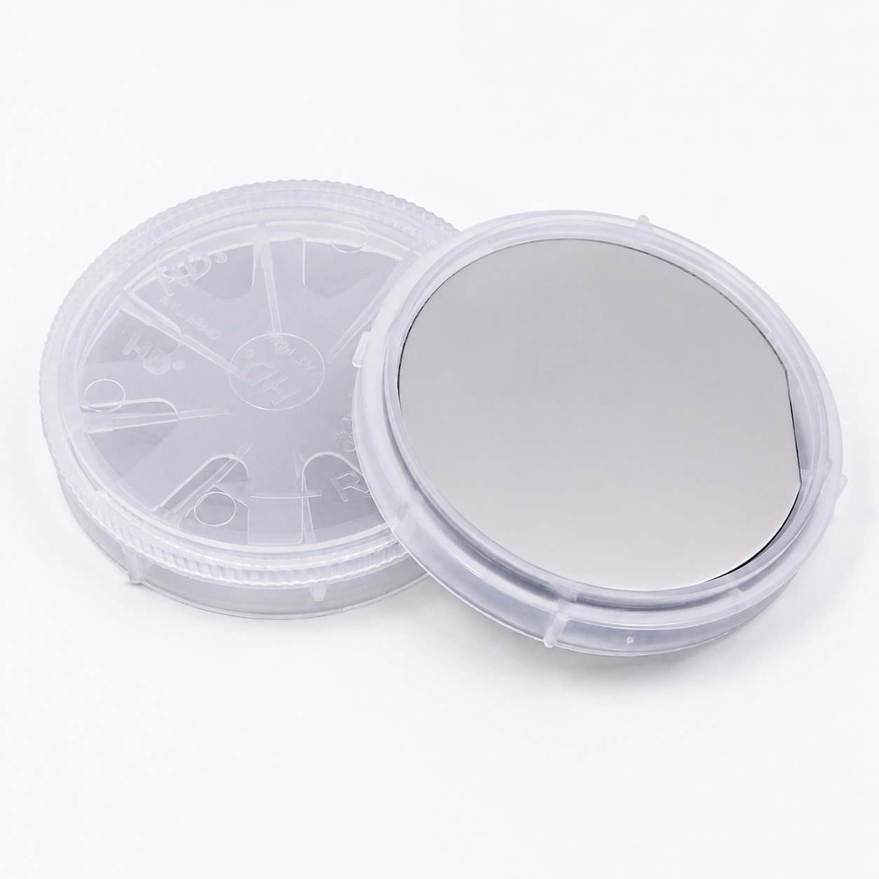
Select a diameter to review the corresponding published specification set.
High-speed optical receivers, mmWave HEMTs | Typical Structure: PIN/APD Detector HEMT Channel | Key Properties: High electron mobility Absorption at 1.3-1.55µm
DFB Lasers, EMLs, Electro-absorption modulators (EAM), Optical amplifiers | Typical Structure: Multiple Quantum Well Laser Structures | Key Properties: Direct bandgap Tunable wavelength
ultra-high-speed HEMTs and HBTs | Typical Structure: 2DEG heterostructure | Key Properties: Better gain Lower noise Higher power efficiency
High-performance MWIR & LWIR Imaging | Typical Structure: T2SL IR Detector Structures | Key Properties: Broad spectral coverage (extendable >14µm)
Mid-IR Lasers for gas sensing | Typical Structure: Quantum Well Laser Structures | Key Properties: Direct bandgap, Mid-IR emission
TPV cells | Typical Structure: PIN structure | Key Properties: High-efficiency energy conversion
5G/6G RF HEMTs, Near-IR Laser Diodes (LDs) | Typical Structure: Quantum Wells, Heterostructures | Key Properties: High electron mobility Direct bandgap
RF Power Amplifiers (HBTs) | Typical Structure: HBT Structures | Key Properties: High breakdown voltage High efficiency
mmWave LNAs, High-speed switches | Typical Structure: pHEMT Structures | Key Properties: Very high electron mobility & velocity
High-brightness Red, Yellow, Orange light emitting diodes (LEDs) | Typical Structure: Multiple Quantum Well Structures | Key Properties: Direct bandgap Red-Yellow spectrum
Terahertz photoconductive antennas, Ultra-fast photodetectors | Typical Structure: Low-Temperature Grown GaAs (LTG-GaAs) Layer | Key Properties: Ultra-high resistivity Ultra-fast carrier lifetime
Quick answers on material selection, customization, testing and ordering.
Please provide the substrate material, wafer diameter, crystal orientation, layer structure, layer thickness, composition, doping requirements, quantity and target device.
Yes. If you do not have a finalized layer structure, our technical team can discuss the target device, wavelength, frequency or performance requirements and recommend a suitable epitaxial structure.
Yes. We can customize layer composition, thickness, doping, quantum-well structures, buffer layers, cap layers and superlattice designs.
Technical Inquiry
Share your material, dimensions, specifications, application or project stage. Our team will review your requirements and respond within one business day.
Engineering-led response
Inquiries are routed to the appropriate technical or commercial team.
Address
No. 1389, Lianmei Road, Lianhua Industrial Zone, Tong’an, Xiamen, Fujian 361100, China
Phone


