

In the millimeter-wave bands (W-band: 75–110GHz; E-band: 60–90GHz), the frequency figures of merit (fₜ and fₘₐₓ) of GaN-based HEMTs depend critically on the aspect ratio between gate length (Lg) and gate-to-channel distance (dge). As Lg is scaled down to sub-micron and even hundred-nanometer dimensions, the suppression of short-channel effects requires a simultaneous reduction of dge, which calls for an ultrathin-barrier structure.
Conventional AlGaN/GaN heterojunctions face intrinsic physical limitations in this scenario: when the barrier thickness falls below 10nm, the metal-piezoelectric-polarization-induced two-dimensional electron gas (2DEG) sheet density decays exponentially, leading to severe channel conductance degradation. In contrast, InAlN ternary alloys with an In composition of approximately 17%–18% are lattice-matched to GaN, and their spontaneous and piezoelectric polarizations are significantly stronger than those of AlGaN of the same thickness. This unique property enables InAlN/GaN HEMT heterojunctions to maintain a high 2DEG density (>10¹³cm⁻²) even with an ultrathin barrier of 5–6nm, providing an ideal material platform to overcome the scaling bottleneck for millimeter-wave devices.
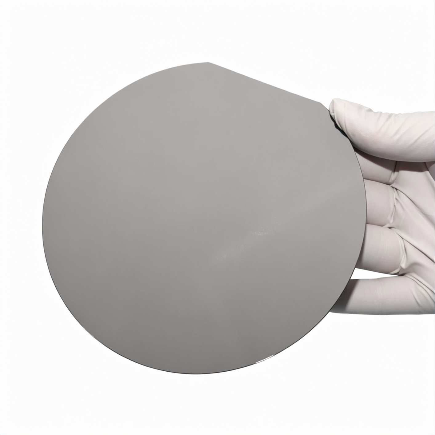
Power Wafertech Group has developed InAlN/GaN heterojunction epitaxial wafer on silicon(Si), sapphire, and silicon carbide(SiC) substrates using metal-organic chemical vapor deposition (MOCVD) technology. We support customized designs from lattice-matched compositions to high-In-content formulations, tailored for different frequency and power application scenarios. Taking the sapphire-based InAlN/GaN HEMT epitaxial structure as a specific example:
1. Sapphire-based InAlN/GaN HEMT Epitaxial Specifications
| Epi Layer | Material | Thickness |
|---|---|---|
| Cap Layer | GaN | * |
| Barrier Layer | InAlN | * |
| Interface Layer | AlN | 1.1nm |
| Channel | GaN | * |
| Buffer | * | * |
| Substrate | Sapphire | – |
Compared to an AlGaN barrier of the same thickness, the InAlN/GaN wafer exhibits superior channel charge density enhancement under the same gate-control distance, which directly translates into improved transconductance and cutoff frequency potential.
2. Phase-Separation Suppression and Strain Engineering in InAlN Epitaxy
MOCVD growth of InAlN faces thermodynamic miscibility-gap limitations, with an intrinsic phase-separation tendency in In-rich regions (xIn> 0.5). To avoid secondary-phase precipitation and ensure structural integrity of the barrier layer, we have integrated the following core measures in our process scheme:
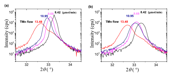
(1) Coupled control of growth temperature and source flows: By precisely setting the growth temperature window (~706°C) and the TMIn/TMAl molar flow ratio, the In composition is locked within the lattice-matched range, thermodynamically avoiding the unstable miscibility-gap region. No secondary-phase diffraction peaks are observed in XRD (0002) rocking curves, confirming single-phase epitaxy.
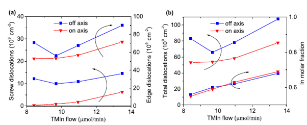
(2) Substrate orientation engineering: We have verified the effects of both on-axis and 4° off-axis sapphire substrates. On-axis substrates are favorable for reducing overall threading dislocation density, while off-axis substrates can suppress hillock formation on N-polar surfaces.
(3) In-situ Si₃N₄ passivation layer integration: An optional in-situ Si₃N₄ dielectric layer with a thickness of about 5nm can be integrated. This thin layer can serve either as a MIS gate dielectric or as a surface passivation layer, effectively pinning surface states and reducing RF losses. Due to its very thin thickness, this dielectric layer can be removed by selective dry etching or directly penetrated for ohmic contact formation, making it compatible with various customer fabrication process routes.
3. Device-Level Performance Verification of InAlN/GaN HEMTs
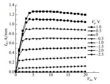
Sakharova et al. (2018) fabricated HEMT devices (Lg = 0.5μm, Wg = 200μm, source-drain spacing = 4μm) based on InAlN/AlN/GaN on-sapphire epiwafers. Pulsed I-V (pulse width 250ns) and DC test results are as follows:
Maximum saturated drain current (Id,max): ≥1.27A/mm
Peak transconductance (gm,max): ≥450mS/mm
Threshold voltage uniformity: within-wafer standard deviation of Vth <0.15V, meeting batch device consistency requirements.
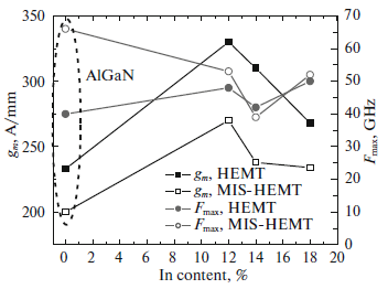
Small-signal RF testing (Vds = 15–20V, Id = 0.1A/mm) shows that, compared to AlGaN reference samples of the same structure, the fmax of InAlN/GaN samples increases significantly with the introduction of In composition. This performance advantage is attributed to the improved gate aspect ratio and stronger channel confinement under the ultrathin barrier. In addition, the MIS-HEMT version with in-situ Si₃N₄ gate dielectric provides an additional positive shift of 3–4V in threshold voltage, offering flexibility for enhancement-mode device design.
Our company offers epitaxial supply capabilities ranging from R&D-scale small batches to production-scale engineering lots, with flexible parameter adjustments based on the target frequency band and power level of the customer’s devices. For custom epitaxial solutions, please contact our technical sales team.
References:
1. Hasenöhrl, S., Blaho, M., Dobročka, E., Gucmann, F., Kučera, M., Nádaždy, P., ... & Kuzmík, J. (2023). Growth of N-polar In-rich InAlN by metal organic chemical vapor deposition on on-and off-axis sapphire. Materials Science in Semiconductor Processing, 156, 107290.
2. Sakharov, A. V., Lundin, W. V., Zavarin, E. E., Zakheim, D. A., Usov, S. O., Tsatsulnikov, A. F., ... & Velikovskiy, L. E. (2018). Ultrathin barrier InAlN/GaN heterostructures for HEMTs. Semiconductors, 52(14), 1843-1845.
Discuss a substrate requirement with our team
Power Wafertech supplies high-quality semiconductor wafers and epitaxial solutions tailored to your device specifications. Reach out to explore substrate and epiwafer options for your next project.
Contact Our Team