

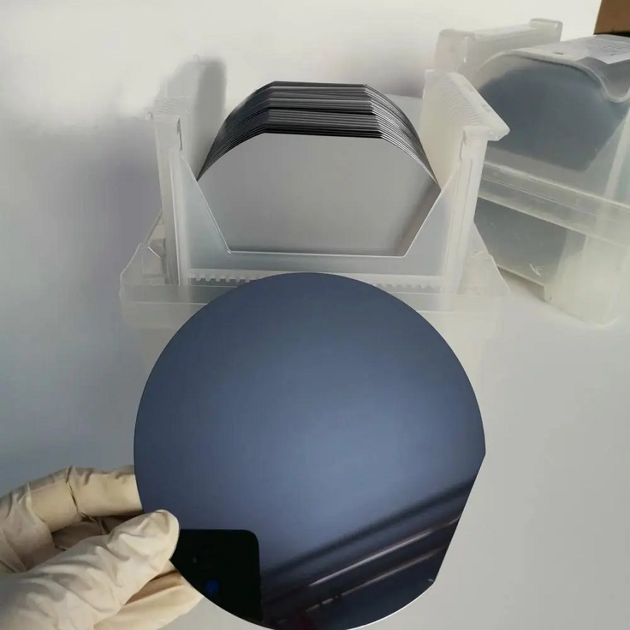
In semiconductor physics, microelectronics, and materials science research, the accuracy of experimental data and the yield of device fabrication are strongly influenced by the surface cleanliness of semiconductor wafers. Residual organic contaminants, metallic ion contamination, or particle adhesion can lead to non‑uniform thin‑film growth, abnormal interface state densities, or even experimental failure.
As a professional semiconductor materials supplier, Power Wafertech Group (PWG) provides silicon wafer products tailored to research requirements. For further details, please contact our sales team. This article describes the industry‑standard RCA cleaning process, offering a reference for laboratory personnel to achieve atomically clean silicon wafer surfaces in experimental work.
1. Definition and Necessity of Cleaning
In integrated circuit manufacturing, cleaning steps account for approximately one-quarter of the total process flow. For research applications, the objectives of cleaning are to remove contaminants and obtain a chemically uniform, damage-free surface.
Contaminants on silicon wafer surfaces fall into four categories:
Organic contaminants: including photoresist residues, oils, and skin secretions, impeding chemical reactions and thin-film deposition.
Particulate contaminants: including dust or inorganic particles, which will cause local shorts or increase surface roughness.
Metallic impurities: including heavy metal ions such as Fe, Cu, and Al, which can introduce deep-level traps in silicon and affect carrier lifetime.
Native oxide layer: SiO ₂ layer formed in the air, altering the surface chemical activity and electrical properties of silicon wafers.
2. Standard RCA Cleaning Procedures and Critical Process Parameters
The RCA cleaning process is the standard method currently used for removing surface contaminants from silicon wafers. The process consists of six steps: SPM cleaning, SC-1 cleaning, deionized water overflow rinsing, DHF cleaning, SC-2 cleaning, and drying. Each step targets specific types of contaminants. The formulations, process conditions, and functions of each step are summarized in the table below:
| Step | Name | Typical Ratio (volume ratio) | Temperature | Time | Core Function | Subsequent Treatment |
|---|---|---|---|---|---|---|
| 1 | SPM cleaning | H₂SO₄:H₂O₂ = 2:1 – 5:1 | 120–150°C | 10–20min | Oxidative decomposition of organics and photoresist residues | DIW overflow rinse 5–10min |
| 2 | SC-1 cleaning | NH₄OH:H₂O₂:H₂O = 1:1:5 | 70–80°C | 5–15min | Particle removal (electrostatic repulsion), saponification of organics, formation of hydrophilic oxide layer | DIW overflow rinse 5–10min |
| 3 | DIW overflow rinse | High-purity deionized water | Room temperature | 5–10 min | Remove residual precursor chemical reagents to prevent secondary pollution caused by acid-base neutralization reactions | — |
| 4 | DHF cleaning | HF:H₂O = 1:50 – 1:100 | Room temperature | 30–60s | Removal of native oxide layer and metals (Al, Fe, etc.) adsorbed on the oxide; hydrogen passivation of silicon surface | DIW overflow rinse 3–5 min |
| 5 | SC-2 cleaning | HCl:H₂O₂:H₂O = 1:1:6 | 70–80°C | 5–10min | Conversion of metal ions (Fe, Al, Cu, Zn, etc.) into soluble chloride complexes for removal from the surface | DIW overflow rinse 5–10min |
| 6 | Drying | IPA vapor drying/N₂ spin-dry/Marangoni drying | — | — | Ensure a water-stain-free and particle-free surface | — |
Process notes:
SPM cleaning: This is an exothermic reaction and must be conducted in a fume hood. After this step, a chemical oxide layer is formed on the silicon surface.
SC-1 cleaning: In the alkaline environment, both the silicon surface and particles carry negative charges, generating electrostatic repulsion that detaches particles from the surface; H₂O₂ simultaneously oxidizes and decomposes organic substances.
DIW overflow rinse: Must be performed before transitioning between acidic and alkaline environments to prevent residual chemicals from undergoing neutralization reactions, which could cause re-deposition of contaminants.
DHF cleaning: This step effectively removes metallic impurities adsorbed on the native oxide layer and results in hydrogen passivation of the silicon surface.
SC-2 cleaning: In the acidic environment, H₂O₂ acts as an oxidant, while hydrochloric acid provides chloride ions to convert metals into soluble chloride complexes.
Drying: Commonly used methods include isopropyl alcohol (IPA) vapor drying, N₂ spin-drying, or the Marangoni drying technique.
Operational precautions:
Specific treatment times should be adjusted according to the degree of contamination and wafer size.
H₂O₂ is prone to decomposition; all solutions used in each step should be prepared fresh immediately before use.
Containers employed during the process should be made of quartz or PTFE to avoid metallic contamination.
All chemical operations must be carried out in a fume hood, and operators are required to wear chemically resistant gloves and protective goggles.
3. Products and Services
PWG offers the following products and support:
Material supply: offer prime / research / dummy-grade silicon wafers compliant with SEMI standards, covering various crystal orientations (e.g., <100>, <111>), doping types (P-type, N-type), and resistivity ranges, with sizes from 2 inches to 12 inches. Oxidized silicon wafers are also available.
Technical support: Consulting on cleaning process adaptation and recommendations on substrate material selection for special specifications.
Clean-room packaging: Vacuum or nitrogen-purged sealed packaging performed in an ISO Class 4 (equivalent to Class 10) cleanroom environment to prevent secondary contamination during transport. Each batch is accompanied by a quality analysis report.
Discuss a substrate requirement with our team
Power Wafertech supplies high-quality semiconductor wafers and epitaxial solutions tailored to your device specifications. Reach out to explore substrate and epiwafer options for your next project.
Contact Our Team