

With the explosive growth of big data, cloud computing, and artificial intelligence, global data traffic is increasing exponentially, imposing ever-higher demands on transmission rates and bandwidth. Silicon photonics is regarded as the mainstream technology for next-generation on-chip interconnects due to its broad bandwidth, high speed, and low power consumption. However, silicon’s indirect bandgap makes efficient light emission inherently difficult, driving the search for luminescent materials that can be directly integrated onto silicon platforms.
III-nitride semiconductors (e.g., GaN, InGaN, AlGaN) feature direct and tunable bandgaps covering ultraviolet to infrared wavelengths, and have already demonstrated outstanding performance in LEDs and laser diodes (LDs). In particular, GaN-based laser diodes grown on silicon substrates (GaN-on-Si LD) , especially those emitting around 405 nm (violet) , are highly promising on-chip light sources for silicon photonics. This wavelength band enables critical applications in visible-light communications, underwater communication, atomic clocks, high-density optical storage, and sensing—making the violet LD a key enabler for next-generation photonic integration.
1. Performance Bottlenecks of Violet LDs and Superlattice Barrier Optimization
Despite the demonstration of room-temperature electrically driven lasing in GaN-based violet LDs, device performance remains constrained by several physical factors that are of particular interest to academic researchers:
Low hole injection efficiency: The hole mobility in Mg-doped p-type layers is far lower than electron mobility, and holes have a large effective mass, leading to non-uniform carrier distribution in the active region and limiting radiative recombination.
Electron leakage: Under high injection currents, electrons readily surmount the electron-blocking layer (EBL) and leak into the p-region, causing non-radiative recombination and increasing threshold current.
Polarization-induced band bending: Strong spontaneous and piezoelectric polarization effects in GaN-based materials generate built-in electric fields at quantum-well/barrier interfaces, tilting the energy bands and reducing electron–hole wavefunction overlap, which degrades luminous efficiency.
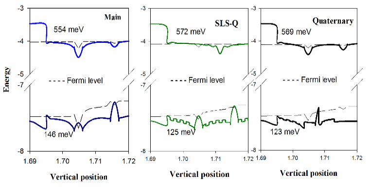
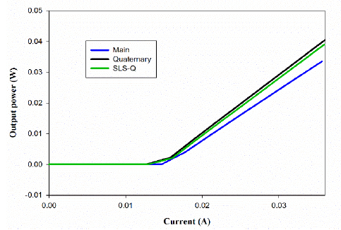
To address these challenges, researchers have explored novel barrier structures to replace conventional GaN barriers. Alahyarizadeh et al. (2022) numerically compared three schemes: GaN barriers, AlGaN barriers, and AlGaN/InGaN superlattice barriers. Their key findings:
The AlGaN barrier raises the effective electron barrier from ~400meV to 569meV while lowering the hole effective barrier to 123meV, enhancing hole injection and electron confinement—yet it does not significantly reduce threshold current.
The AlGaN/InGaN superlattice barrier effectively suppresses the internal electric field due to reduced polarization charges at the superlattice interfaces and alleviates band bending. Simulations show that this structure lowers the threshold current from 16.6mA to 12.9mA (a ~22% reduction) while simultaneously improving output power, differential quantum efficiency, and slope efficiency.
Physical mechanism: The superlattice barrier forms a higher conduction-band barrier to block electron overflow, while lowering the valence-band barrier to facilitate hole injection, thus significantly boosting the radiative recombination rate in the active region. This optimization direction provides clear experimental guidance for epitaxial wafer design.
2. Violet Laser Diode Epitaxial Wafer Specifications
Power Wafertech Group offers GaN-based laser diode epiwafers targeting the violet band, with a dominant wavelength of 405nm. We support customised epitaxial structure designs to meet diverse research requirements, including variations in thickness, composition, and doping profiles. Key product parameters are summarized below:
| Epi No. | Material | Thickness | Al(%) | In(%) | Doping |
|---|---|---|---|---|---|
| 8 | Contact layer | 10nm | * | ||
| 7 | p-GaN | * | Mg: * | ||
| 6 | AlGaN | * | * | * | |
| 5 | InGaN | * | * | * | |
| 4 | MQW | * | * | * | * |
| 3 | InGaN | * | * | * | |
| 2 | AlGaN | * | * | * | |
| 1 | n-GaN | * | Si: * | ||
| 0 | Si Substrate |
3. Frequently Asked Questions from Research Customer
Q1: What is the composition and specific Mg doping concentration of the contact layer in the violet LD epiwafer? Given the precise thickness control of MOCVD, is there a theoretical design thickness?
A: Composition & doping: The contact layer in the LD epiwafer is a p++ layer with an extremely high Mg doping concentration; the exact value depends on the specific design and can be tailored.
Thickness: Yes, a theoretical design thickness exists. For detailed values, please contact our sales team.
Q2: Is the lasing wavelength of the GaN laser diode exactly 405nm?
A: 405nm is our customary designation for this band. The actual lasing wavelength typically falls in the range of 400–415nm, with the exact value varying slightly depending on material growth details and device fabrication processes.
Q3: What method does you currently use to cleave GaN-on-Si material into bar strips? We previously processed GaAs materials by: thinning to a certain thickness → scoring along the cleaving direction with a cleaving machine → rolling and breaking. However, given that GaN is much harder than GaAs and the silicon substrate appears to lack a well-defined natural cleavage plane, does the same cleaving method work for silicon-based GaN epiwafers? Or do you recommend an alternative approach?
A: This process is equally effective for silicon-based GaN epiwafers and can be performed as described.
Q4: Can you provide lasing performance data (L-I-V curves, etc.) based on the LD epitaxy after device fabrication?
A: Specific lasing performance data (e.g., threshold current, output power) depend on the final device process. We recommend contacting our sales team directly for further details.
The AlGaN/InGaN superlattice barrier has demonstrated significant improvements in GaN‑based violet LDs, offering a viable path toward high‑performance on‑chip light sources for silicon photonics. Power Wafertech Group provides customisable epiwafers with precise control over polarisation engineering, doping profiles, and band structure, supporting academic and research institutions in exploring innovative device concepts—from material growth to full device fabrication.
Reference:
Alahyarizadeh, G., Amirhoseiny, M., & Khorsandi, M. (2022). Performance enhancement of deep violet InGaN double quantum wells laser diodes with quaternary superlattice barriers structure. Journal of Renewable Energy and Environment, 9(1), 106-111.
Discuss a substrate requirement with our team
Power Wafertech supplies high-quality semiconductor wafers and epitaxial solutions tailored to your device specifications. Reach out to explore substrate and epiwafer options for your next project.
Contact Our Team