
01
MOS & Gate Dielectrics
Thin dry thermal SiO2 layers act as high-quality gate dielectrics and insulators. Ideal for MOSFETs, MOS capacitors, analog devices, and sensor fabrication.

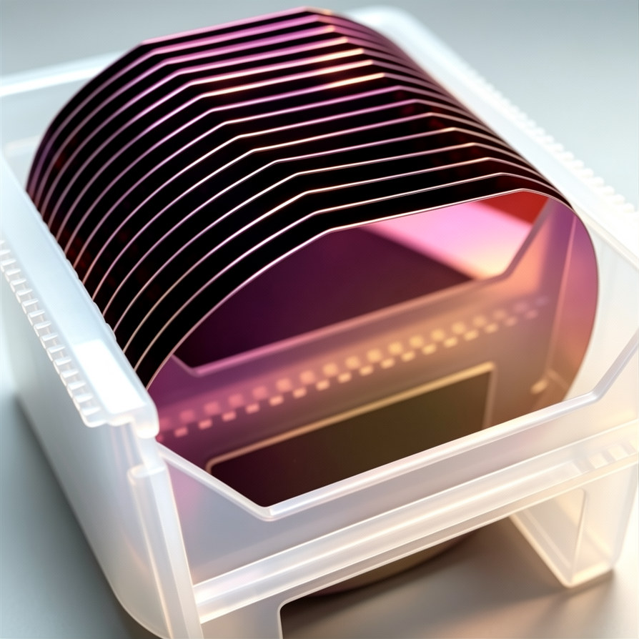
Select a wafer type to view detailed specs
Thin dry thermal SiO2 layers act as high-quality gate dielectrics and insulators. Ideal for MOSFETs, MOS capacitors, analog devices, and sensor fabrication.
Thicker SiO2 layers provide electrical isolation between device structures and protective surface passivation. Essential for power ICs, high-voltage devices, and RF device isolation.
Thermal oxide layers function as insulation, structural, or sacrificial layers in MEMS fabrication. Suitable for pressure sensors, microstructures, and silicon micromachining.
SiO2 provides a highly reliable hard mask for critical semiconductor processing steps. Used extensively in dopant diffusion, ion implantation, and etching processes.
Quick answers on material selection, customization, testing and ordering.
A silicon dioxide (SiO2) wafer consists of a silicon substrate with a precisely controlled thermal oxide layer grown on its surface. It is widely used for electrical insulation, surface passivation, hard masking, and gate dielectric fabrication.
Dry oxidation produces a dense, high-quality oxide with superior electrical properties, preferred for thin gate oxides. Wet oxidation offers a higher growth rate and is typically used for thicker SiO2 layers, such as field oxides and masking layers.
Our thermal oxidation processes deliver excellent wafer-level uniformity, typically ≤ 3% (depending on oxide thickness and wafer size). This ensures highly repeatable device performance and yield.
Please provide: Wafer size, crystal orientation, doping type, resistivity, target SiO2 thickness, oxidation method (Dry/Wet), oxidation side (Single/Double), and order quantity.
Technical Inquiry
Share your material, dimensions, specifications, application or project stage. Our team will review your requirements and respond within one business day.
Engineering-led response
Inquiries are routed to the appropriate technical or commercial team.
Address
No. 1389, Lianmei Road, Lianhua Industrial Zone, Tong’an, Xiamen, Fujian 361100, China
Phone


