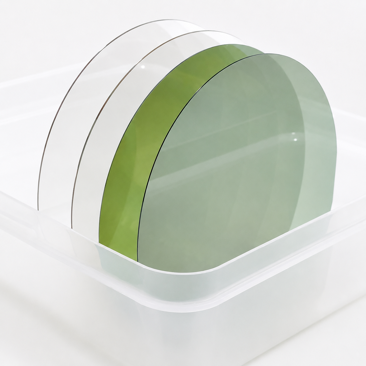
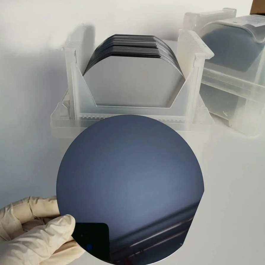
Silicon Wafer RCA Standard Cleaning
Learn silicon wafer RCA cleaning steps and key parameters. PWG supplies 2–12" prime/research/dummy grade Si wafers with technical support
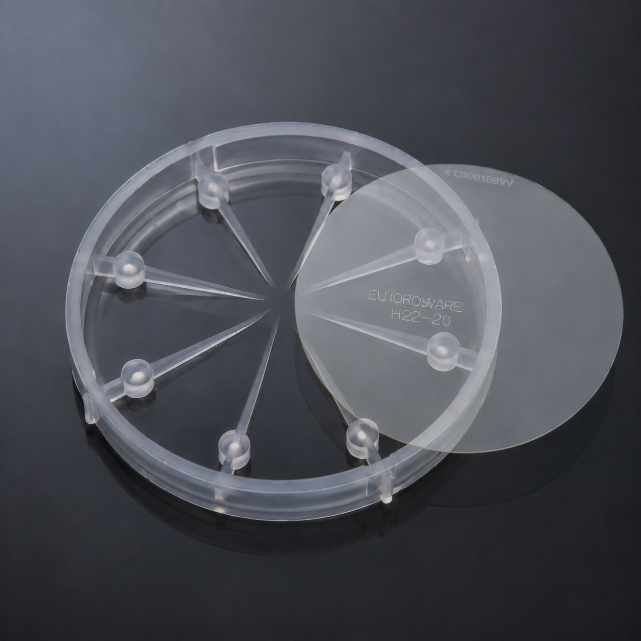
8-inch SiC substrates are moving from pilot to mainstream. Explore 2026 supply, pricing and epitaxy implications for power device makers.
1788243588
Read ArticleLearn silicon wafer RCA cleaning steps and key parameters. PWG supplies 2–12" prime/research/dummy grade Si wafers with technical support
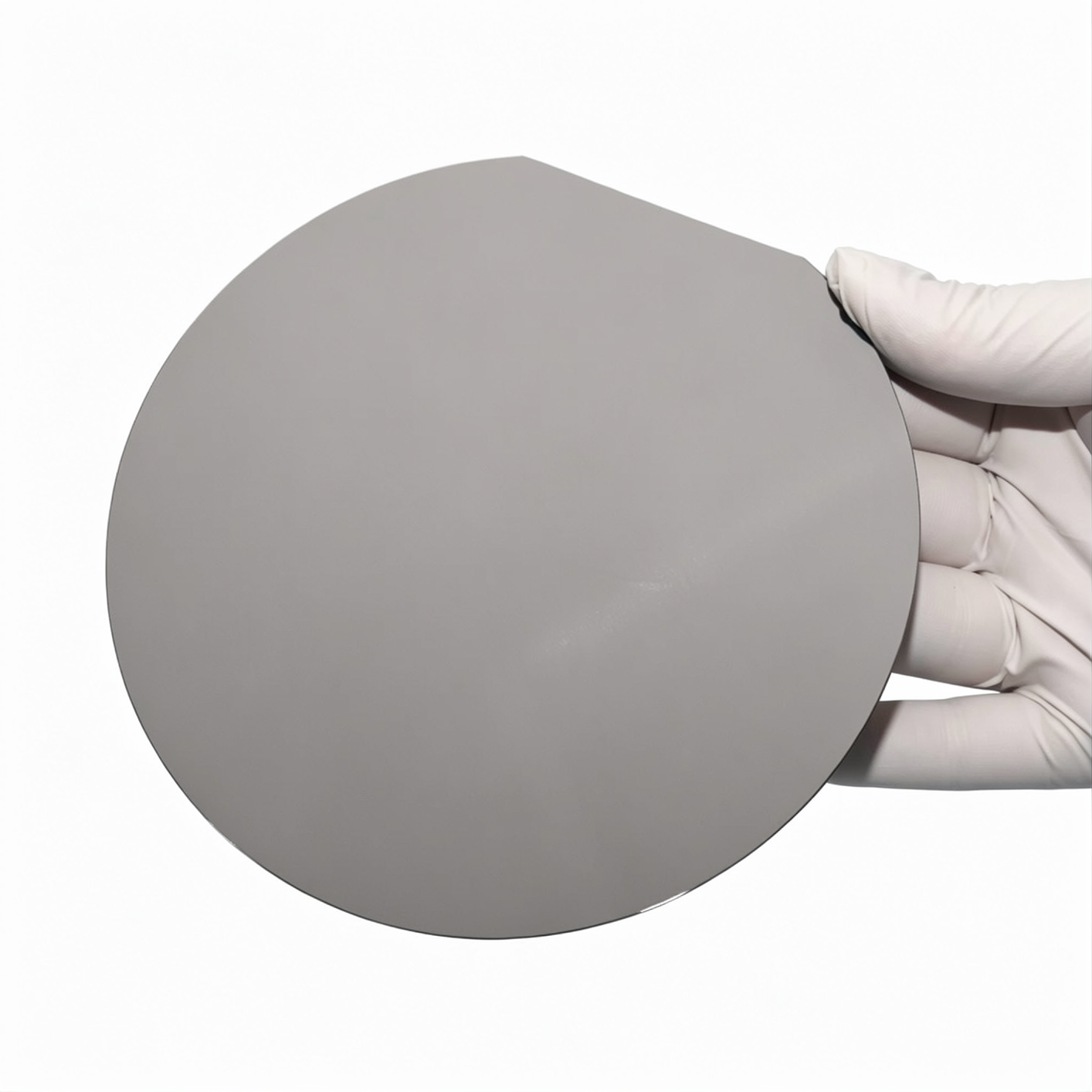
Offer various commercial epitaxy GaN photodetector wafers with customizable structures, covering different substrates and application requirements
Custom InAlN/GaN HEMT epiwafers on sapphire, SiC, and Si substrate, with high-density 2DEG, ideal for Millimeter-Wave Applications
High-performance GaN based violet laser diode epiwafers supplied are grown Si substrate by MOCVD method with multi quantum wells for low threshold current.
As a professional silicon wafer supplier, PWG masters the control of Crystal Originated Particle (COP) defects, ensuring crystal integrity & yield for your ULSI devices
Discover PWG's 4H-SiC PIN diode epiwafers with optimized epilayer design, ensuring high reliability for power electronics
Share a specification, request evaluation samples or speak with our engineering team about your application.
Request a Quote