InAs Wafer & InAs Substrate Supplier | Power Wafertech Group

III-V Compound Wafers

InAs Wafer

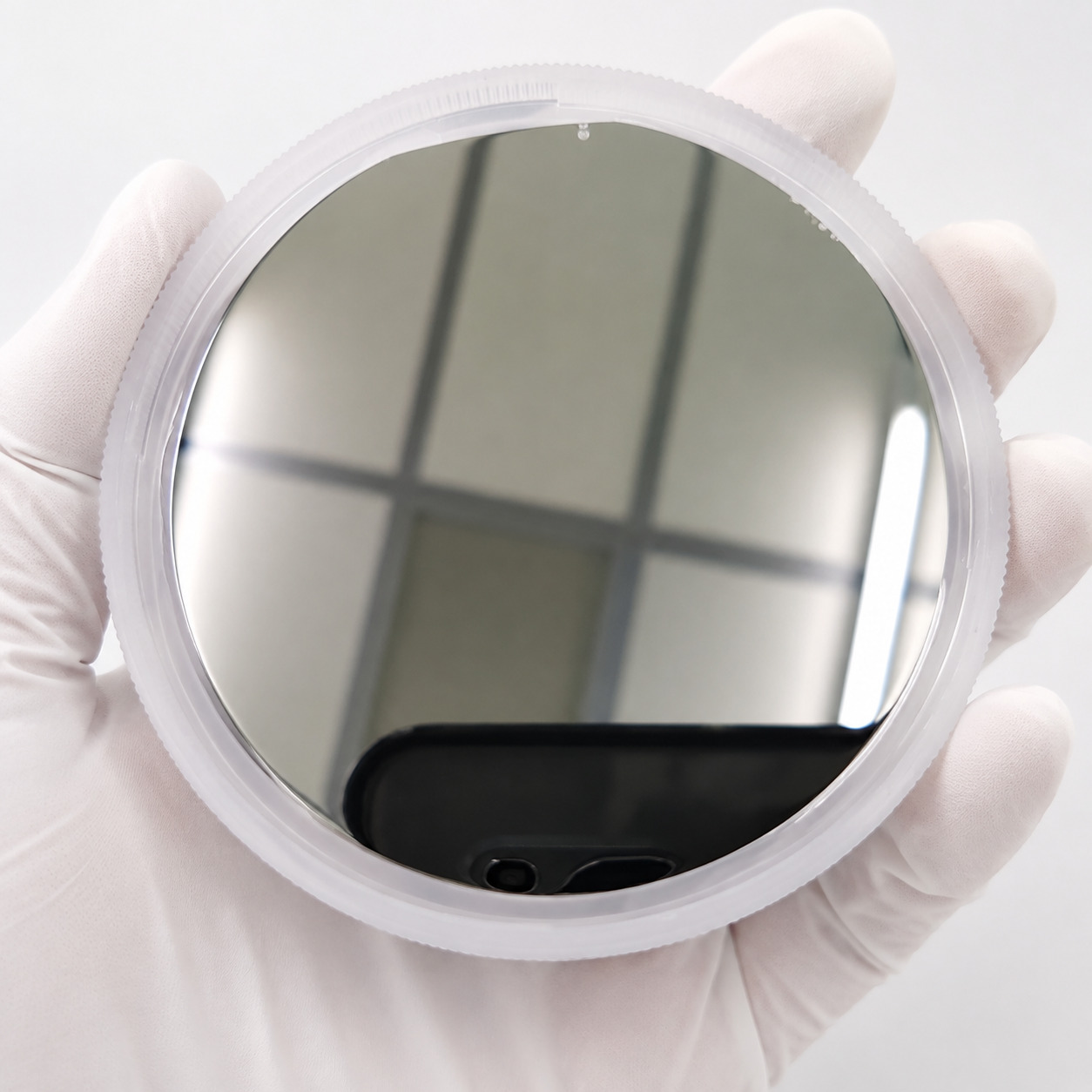
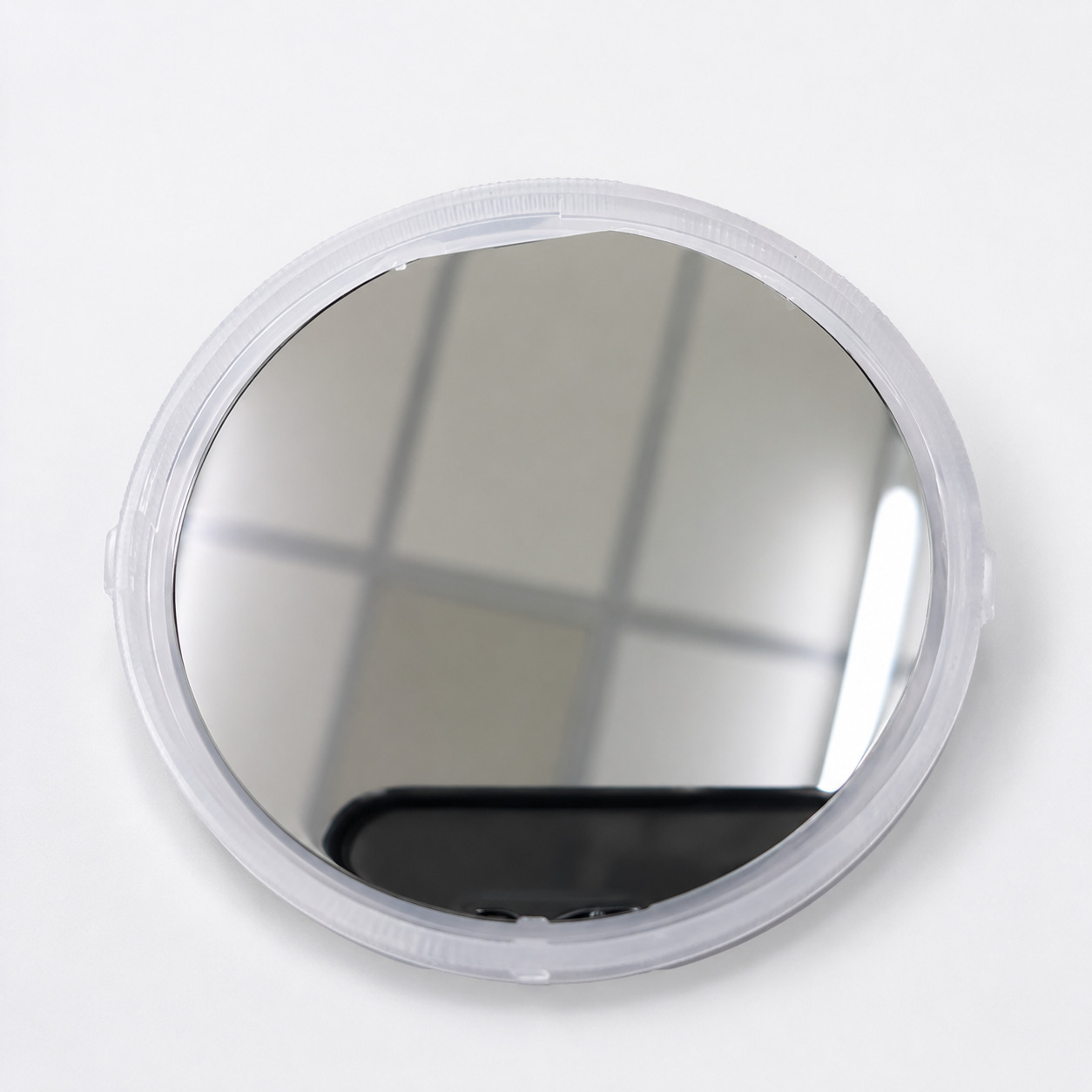
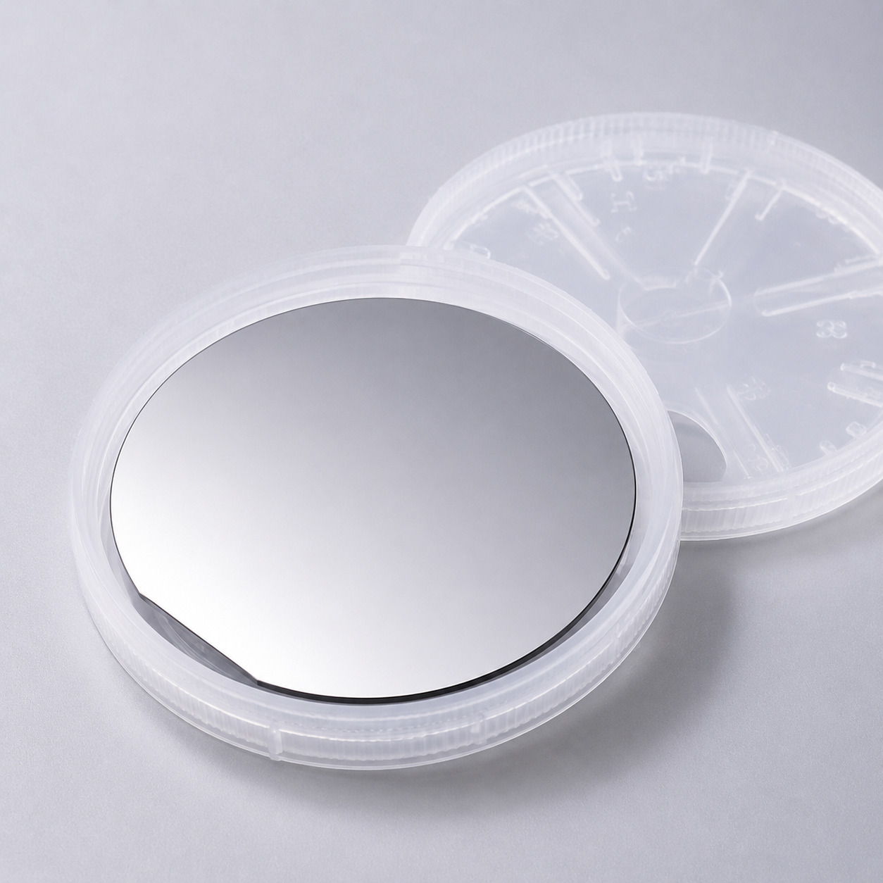
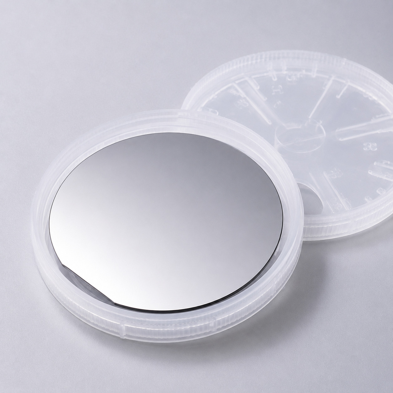
Power Wafertech Group supplies indium arsenide (InAs) substrate wafers for infrared detection, high-mobility electronics and advanced III-V semiconductor research. Available options include N-type and P-type InAs, with selected wafer diameters, crystal orientations and surface finishes for device fabrication and epitaxial growth.
  • Size — 2", 3" and 4"
  • Orientation — (100), (111)
  • Conduction type — N-type (S / Sn-doped) and P-type (Zn-doped)
  • Surface finished — SSP / DSP, epi-ready
  • Packaging — Single or multi‑wafer cassette, vacuum sealed
Detailed Specifications

Specifications by wafer type.

Select a wafer type to view detailed specs

Parameter 2”(50.8mm) InAs Substrate
Conduction Type N-Type P-Type
Dopant S / Sn Zn
Orientation (100) / (111) (100) / (111)
Thickness 500±25um 500±25um
TTV <10um <10um
Bow <10um <10um
Warp <12um <12um
Electron Mobility 6,000–20,000 or ≥20,000 cm²/V·s 100–400 cm²/V·s
Carrier Concentration 5 × 10¹⁵–1 × 10¹⁰ cm⁻³ (1–10) × 10¹⁵ cm⁻³
EPD ≤50,000 cm⁻² ≤30,000 cm⁻²
Surface Finish SSP / DSP, epi-ready SSP / DSP, epi-ready
Flat SEMI standard SEMI standard
Packaging Single wafer cassette, vacuum sealed Single wafer cassette, vacuum sealed
Applications

Where this wafer delivers value

01

Infrared Detectors & Sensors

InAs is ideal for mid-wave infrared (MWIR) detection. It is widely used in photodetectors, IR sensors, and focal plane arrays (FPAs) for applications such as gas sensing, spectroscopy, and thermal imaging.
02

High-Mobility Electronics

Featuring ultra-high electron mobility, InAs enables advanced high-speed electronics. Typical devices include high-mobility transistors (HEMTs) and Hall-effect sensors, supporting quantum device research and high-frequency applications.

03

III-V Epitaxy

InAs provides a versatile platform for MBE and MOCVD growth of narrow-bandgap heterostructures. It supports the epitaxial development of InAs/GaSb Type-II superlattices (T2SL) and InAsSb alloys for advanced MWIR/LWIR devices.

FAQ

Common questions about this product

Quick answers on material selection, customization, testing and ordering.

Indium arsenide (InAs) wafers are used in infrared detection, high-mobility electronic devices and III-V semiconductor research. Typical applications include infrared photodetectors, Hall sensors, high-speed transistor structures and epitaxial material development.

The appropriate InAs substrate depends on the epitaxial material system, growth process, crystal orientation, surface condition and device structure. Specify your growth requirements and surface acceptance criteria when requesting a quotation.

N-type InAs is commonly selected for applications that require high electron mobility.

Submit your required specifications, quantity and intended application through the technical inquiry form. You can also attach a specification sheet or drawing to help us assess your requirements.

Technical Inquiry

Speak to Engineers About Your Wafer Needs

Share your material, dimensions, specifications, application or project stage. Our team will review your requirements and respond within one business day.

Engineering-led response

Inquiries are routed to the appropriate technical or commercial team.

Address

No. 1389, Lianmei Road, Lianhua Industrial Zone, Tong’an, Xiamen, Fujian 361100, China

File Upload
Emailvictorchan@powerwafertech.com Phone+86-592-5633652